
The global semiconductor industry's pursuit of wider bandgap materials has positioned Silicon Carbide (SiC) as a cornerstone for next-generation power electronics. Leading 4 inch SiC Substrates Manufacturers are at the forefront of this supply chain, which is fundamentally built upon several critical segments: substrate → epitaxial wafer → device fabrication (chips & modules) → end-use applications.
Substrate (SiC Wafer) Manufacturing:
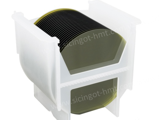
The production of high-quality Conductive and semi-insulating SiC wafers, the foundational material supplied by 4 inch SiC substrates manufacturers, is a sophisticated, multi-step process. It begins with the synthesis of SiC single crystals, predominantly using the Physical Vapor Transport (PVT) method. In this process, source materials are sublimated at extreme temperatures (>2000°C) and recrystallized onto a seed crystal. The resulting cylindrical ingot then undergoes precision machining: it is sliced into thin wafers, which are subsequently ground, lapped, and polished. The final output is a pristine, transparent or semi-transparent 4-inch (or larger) SiC wafer with an ultra-low roughness and minimal sub-surface damage, ready for epitaxial growth.
At present, methods for preparingSiC single crystals include the seeded sublimation method, high-temperature chemical vapor deposition (HTCVD), and liquid-phase epitaxy (LPE). However, the latter two methods are not yet mature. The seeded sublimation method, also known as the physical vapor transport (PVT) method, involves sublimating carbon and silicon powders at temperatures exceeding 2000°C to form gaseous substances such as Si atoms, Si₂C molecules, and SiC₂ molecules. Driven by a temperature gradient, these gaseous substances are transported to a cooler Silicon Carbide seed crystal to form 4H-SiC crystals. By controlling parameters such as temperature field and gas flow in the PVT process, specific 4H-SiC crystal types can be grown.
SiC Epitaxial Materials:
Unlike traditional silicon power device manufacturing processes, Silicon Carbide power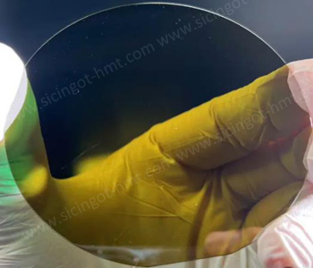 devices cannot be directly fabricated on SiC single-crystal materials. High-quality epitaxial materials must be grown on conductive single-crystal substrates, and devices are manufactured on these epitaxial layers. Currently, HMT can provide 4inch to 8inch SiC Epitaxy wafers with N type and P type epi layers and support customized. the primary epitaxial technology is chemical vapor deposition (CVD), which achieves epitaxial growth of Silicon Carbide with specific thicknesses and doping through step-flow growth. With increasing requirements for SiC power device manufacturing and voltage ratings, SiC epitaxial materials are evolving toward low-defect and thick epitaxial layers. In recent years, the quality of thin SiC epitaxial materials (below 20 μm) has continuously improved, with micropipe defects largely eliminated. As epitaxial growth technology advances, epitaxial layer thickness has increased from a few micrometers or tens of micrometers in the past to the current tens or even hundreds of micrometers.
Devices:
SiC semiconductor power devices mainly include diodes and transistors. Diodes primarily include junction barrier Schottky diodes (JBS), PiN diodes, and merged PiN Schottky diodes (MPS). Transistors mainly include metal-oxide-semiconductor field-effect transistors (MOSFETs), bipolar junction transistors (BJTs), junction field-effect transistors (JFETs), insulated-gate bipolar transistors (IGBTs), and gate turn-off thyristors (GTOs).
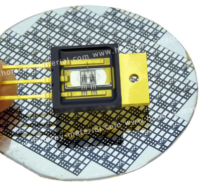 SiC-MOSFET is a highly focused device in SiC power electronics research. For SiC MOSFETs, the N⁺ source region and P-well doping are achieved through ion implantation, followed by annealing activation at 1700°C. Another critical process is the formation of the SiC MOS gate oxide. Silicon IGBTs generally operate at frequencies below 20 kHz. Due to material limitations, high-voltage, high-frequency silicon devices are challenging to achieve. SiC MOSFETs are suitable for a wide voltage range from 600V to 10kV and offer the excellent switching performance of unipolar devices. Compared to silicon IGBTs, SiC MOSFETs do not experience current tailing in switching circuits, resulting in lower switching losses and higher operating frequencies. A 20 kHz SiC MOSFET module can reduce losses by half compared to a 3 kHz silicon IGBT module, and a 50A SiC module can replace a 150A silicon module. SiC MOSFETs offer significant advantages in operating frequency and efficiency.
Overall, SiC devices offer significant advantages, including higher performance and operating voltage, higher operating frequency and temperature, and easier driving.
Power Modules:
To further enhance the current capacity of SiC power devices, module packaging is typically used to integrate and encapsulate multiple chips in parallel. SiC power modules initially developed from hybrid modules combining silicon IGBT chips and SiC JBS diode chips. With the maturation of SiC MOSFET devices, companies such as Wolfspeed, Infineon, Mitsubishi, and Rohm have developed full-SiC power modules consisting of SiC JBS diodes and MOSFETs. Currently, international SiC power module products offer maximum voltage ratings of 3300V, maximum current of 700A, and maximum operating temperature of 175°C. In research and development, full-SiC power modules have achieved maximum current capacities of 1200A and maximum operating temperatures of 250°C, employing technologies such as double-sided chip soldering, new interconnection methods, and compact packaging to enhance module performance.
SiC devices are widely used in fields such as smart grids, rail transportation, electric vehicles, and communication power supplies.
![]() E-mail: kim@homray-material.com ; tina@homray-material.com
E-mail: kim@homray-material.com ; tina@homray-material.com
HMT Gallium Nitride (GaN) Wafer Website: www.ganwafer-hmt.com