

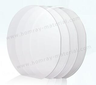
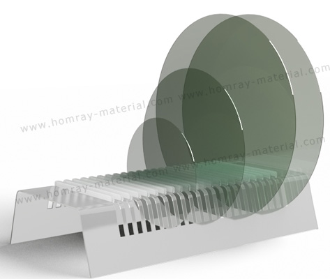
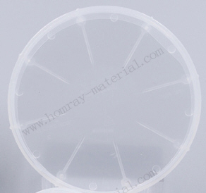
6'' 4H- SiC Wafer Manufacturer(150mm,D)
Grade: D Grade
Type: 4H-N
Dimension:150mm
Thickness:350±25um
Product Description
6 Inch D Grade 4H-N SiC Wafer for Research and Process Development
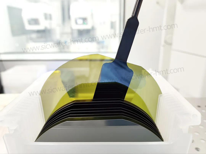
HMT provides 6 inch (150 mm) D Grade 4H-N SiC wafers designed for semiconductor research, process development, equipment testing and non-production applications. The standard wafer thickness is 350±25 μm, while customized specifications can be discussed according to project requirements.
6 Inch D Grade 4H-N SiC Wafer Specifications
| Parameter | Specification |
|---|---|
| Wafer Diameter | 150 mm / 6 inch |
| Crystal Type | 4H-N |
| Grade | D Grade |
| Standard Thickness | 350±25 μm |
| Application | Research, testing, process development |
| Surface | Available according to requirement |
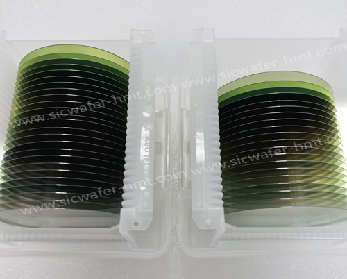
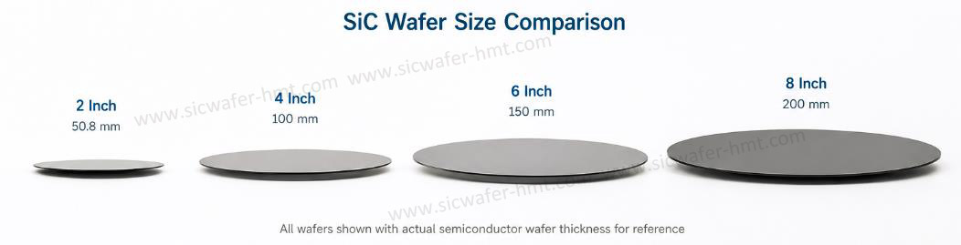
The 150 mm wafer diameter provides a practical platform for laboratories and semiconductor process evaluation that require a larger SiC substrate than 4 inch wafers. With a nominal thickness of 350 μm, this D Grade substrate is suitable for experimental processing, equipment qualification and material evaluation rather than high-volume production.
Why Choose D Grade 4H-N SiC Substrates?
D Grade SiC wafers can be a cost-effective option when production-grade defect specifications are not required. The 4H-N crystal structure and conductive SiC material platform make these wafers suitable for research involving SiC processing, epitaxy development, device experiments and related semiconductor technologies.
For projects requiring production-level substrate specifications, HMT can also provide other 4H-SiC wafer grades and diameters, allowing customers to select the substrate according to device development stage, process requirements and budget.
 Applications of 150 mm D Grade SiC Wafers
Typical applications include SiC process research, wafer handling and equipment testing, semiconductor process development, epitaxy experiments, laboratory device fabrication and material evaluation. The 6 inch format is particularly useful when researchers need a 150 mm substrate platform for process compatibility studies.
HMT supports customized wafer requirements covering diameter, thickness, crystal type, orientation and surface finishing, subject to technical evaluation. Contact HMT with your target specification and application requirements for a suitable wafer configuration.
Related SiC Wafer Resources
For production-grade requirements, see our 4H-SiC substrate wafer solutions. Customers researching the material preparation route can also learn about SiC boule and ingot production before wafer slicing, grinding and polishing.
For a comparison between research and production materials, see our resources on D Grade vs. P Grade SiC wafers and as-cut vs. polished SiC wafers.
FAQ
Q1: What is a 6 inch D Grade SiC wafer?
It is a 150 mm 4H-N SiC substrate intended primarily for research, testing and process development rather than production-grade applications.
Q2: What is the standard thickness?
The listed standard thickness is 350±25 μm.
Q3: Is D Grade SiC suitable for semiconductor research?
Yes. It can be positioned for process research, equipment testing, epitaxy experiments and material evaluation, where production-grade specifications may not be necessary.
Related Products
 E-mail: kim@homray-material.com ; tina@homray-material.com
HMT Gallium Nitride (GaN) Wafer Website: www.ganwafer-hmt.com