

SiC Epitaxial Wafer Manufacturer
Size: 4'' 6''
Type: N-Type/ P-Type
Dopant: Nitrogen/Aluminum
Thickness:0.2~50μm
Product Description
4H-SiC Epitaxial Wafer Manufacturer
HMT supplies 4H-SiC epitaxial wafers for semiconductor device development, process research and epitaxial technology evaluation. Available configurations include 4 inch, 6 inch and 8 inch substrates, with N-type or P-type epitaxial layers and customized layer thickness from 0.2 to 50 μm.
4H-SiC Epi Wafer Specifications

N-Type and P-Type SiC Epitaxial Layers
N-type SiC epitaxial layers use nitrogen doping, while P-type layers use aluminum doping. For N-type epi layers below 20 μm, a 0.5 μm n-type buffer layer at approximately 1E18 cm⁻³ may be applied; for layers of 20 μm or more, a 1–5 μm buffer layer can be used according to the required structure.
P-type SiC epitaxial layers are supplied without a buffer layer under the current specification. Doping concentration and layer thickness should be selected together because not every doping density is available across the complete 0.2–50 μm thickness range.
SiC Epi Wafer for Device Development
A controlled SiC epitaxial layer provides the active semiconductor structure required for developing Schottky diodes, SiC MOSFETs and junction field-effect devices. The 4H-SiC epi platform can also be used for process development, epitaxy evaluation and semiconductor laboratory research.
For 150 mm wafers, the current specification allows a 10 mm edge exclusion, while 76.2 mm and 100 mm wafers use a 5 mm edge exclusion. These parameters should be confirmed together with epi thickness and doping requirements before production.
Production Process Stability

Customized SiC Epitaxial Wafer Solutions
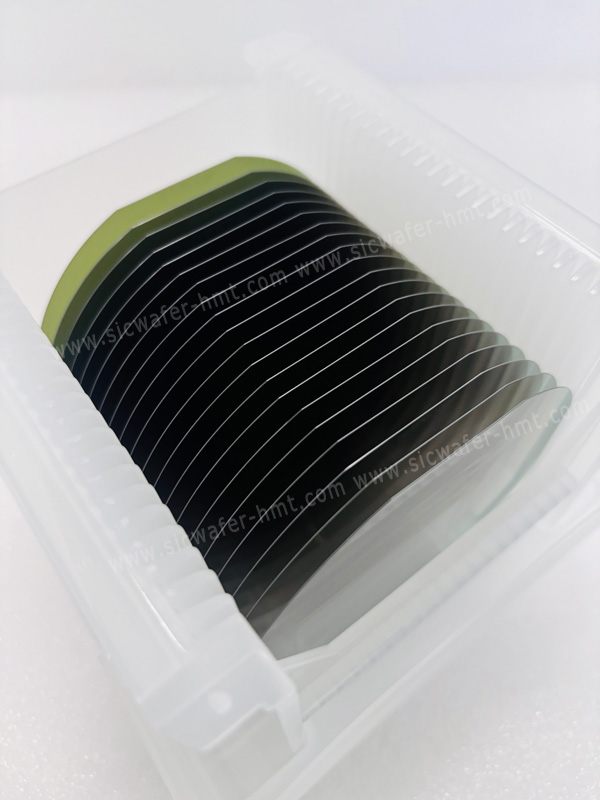 HMT supports customized SiC epi wafer configurations based on wafer diameter, epitaxial layer thickness, conductivity type and doping requirements. Customers can specify the target device structure and process requirements so that the appropriate 4H-SiC substrate and epitaxial layer configuration can be evaluated.
For customers comparing substrate and epitaxial materials, HMT also provides SiC substrate wafers, Epi-Ready SiC wafers and SiC boule/ingot materials, covering different stages of SiC wafer manufacturing and device development.
FAQ
Q1. What is a 4H-SiC epitaxial wafer?
It is a SiC substrate with a controlled epitaxial layer used for semiconductor device development; HMT currently specifies 0.2–50 μm epi thickness.
Q2. What wafer sizes are available?
HMT's product description specifies 4 inch, 6 inch and 8 inch SiC epi wafers. Q3. What is the difference between N-type and P-type SiC epi?
N-type uses nitrogen doping, while P-type uses aluminum doping.
Related Products

 E-mail: kim@homray-material.com ; tina@homray-material.com
HMT Gallium Nitride (GaN) Wafer Website: www.ganwafer-hmt.com